RAM is like the short-term memory of a computer. Find out what role the clock rate and latencies of the RAM play, especially in games.
Current CPUs from AMD and Intel now support RAM with quite fast clock rates: up to 3200MHz with DDR4 RAM and 5600MHz with DDR5. Furthermore, higher clock frequencies are no longer unusual—in these cases, the use of a special profile allows the correct control of the RAM. However, to get these clock rates, you have to adjust a setting in the BIOS (alternative: manual overclocking). We have tested for you how much the clock rate and the latency of the RAM affect the gaming performance of your computer.
How is the maximum supported RAM clock determined?
The stated values for the maximum RAM clock often differ greatly between processor providers and motherboard manufacturers. To ensure the long-term, stable use of a computer, there are specifications for RAM from JEDEC, an organization for the standardization of semiconductors. These concern, for example, the memory clock or the supply voltage. To ensure maximum stability, CPU developers follow these guidelines. In the following table we have compiled for you the latest CPU generations from AMD and Intel, including the RAM clock rates specified by the manufacturers.
| CPU socket | Processor type | Supported RAM clock |
|---|---|---|
| Intel 1700 | Core i5/i7/i9-13000 | 3200 MHz DDR4, 5600 MHz DDR5 |
| Intel 1700 | Core i3/i5/i7/i9-12000, Pentium Gold, Celeron, Core i3/i5-13000 | 3200 MHz DDR4, 4800 MHz DDR5 |
| Intel 1200 | Core i5/i7/i9-11000 | 3200 MHz |
| Intel 1200 | Core i7/i9-10000 | 2933 MHz |
| Intel 1200 | Core i3/i5-10000, Pentium Gold, Celeron G | 2666 MHz |
| Intel 4677 | Xeon w-3400, Xeon w-2400 | 4800 MHz DDR5 |
| Intel 2066 | Core i9-10000 | 2933 MHz |
| AMD AM5 | Ryzen 5/7/9 | 5200 MHz DDR5 |
| AMD AM4 | Ryzen 3/5/7/9 3000, Ryzen 3/5/7 4000, Ryzen 5/7/9 5000 | 3200 MHz |
| AMD AM4 | Ryzen 3/5/7 2000, Ryzen 3/5 3000G | 2933 MHz |
| AMD AM4 | Ryzen 3/5/7 1000, Athlon | 2666 MHz |
| AMD AM4 | A-9000 | 2400 MHz |
| AMD sWRX8 | Ryzen Threadripper PRO 3000, Ryzen Threadripper PRO 5000 | 3200 MHz |
| AMD sTRX4 | Ryzen Threadripper 3000 | 3200 MHz |
On many available motherboards, the maximum RAM clock listed is significantly higher than the above values. The easiest way to clock the RAM higher is to use the so-called “XMP” (Extreme Memory Profile) for Intel, or “EXPO” (Extended Profiles for Overclocking) for AMD.
The manufacturers of memory sticks and motherboards specify higher maximum RAM clock rates in these profiles. This is often accompanied by an increase in the supply voltage. Even if the manufacturers carry out extensive tests for this, you do not receive an absolute guarantee regarding compatibility and stability. This means that if you plan to use a PC 24/7, it is not recommended to activate such a profile. (On AMD motherboards, instead of XMP for DDR4 modules, the name “D.O.C.P.” (Direct Over Clock Profile) is common.)
To get the maximum data throughput, note how many memory channels the motherboard used supports. This number indicates how many working memory blocks the processor, or more precisely the memory controller, can address in parallel. Most motherboards use a dual-channel architecture. In this case, you get a significant performance boost with two RAM modules as opposed to a single memory bar.
RAM: frequency and latencies explained
RAM (Random Access Memory) is something like the short-term memory of your PC. All data and commands that the CPU needs to run a program are stored temporarily in the RAM. The advantage over retrieving data directly from the system memory, such as an HDD or SSD, is the significantly shorter access time and the higher transfer rate.
A memory bar is made up of several memory chips, which in turn consist of millions of small capacitors and transistors. Each memory cell corresponds to one bit and can assume either the status 1 (charged) or 0 (discharged). Since capacitors discharge again, the state is constantly refreshed. The transistors are responsible for restoring or changing the state of a capacitor.
The memory cells are arranged in a grid with rows and columns like in an Excel spreadsheet, which allows the memory controller to address each cell precisely. This is where the name “random access memory” comes from. When accessing a single memory cell, various latency times occur, each of which is specified in clock cycles and thus depends on the frequency of the main memory.
First, the memory controller activates the desired row and sends a read command. This latency is called tRCD = Row-to-Column Delay, which corresponds to the access time from one row to one column. Next comes the actual access time: CL = CAS Latency, which indicates the time span between the read command and the arrival of the desired data or, in other words, the access time to a column. The read row is then deactivated. The entire cycle from activation to reading with data output and deactivation is described by the time tRAS = Active-to-Precharge Time. To reactivate the corresponding row, the time tRP = Row Precharge Time elapses. This is how many cycles must pass before the same row can be accessed again.
The actual elapsed time can be calculated via the frequency of the memory module. Let’s take a DDR4 RAM module with 4000MHz and latencies of CL17-17-17-37 as an example. First we calculate the reciprocal of the effective clock frequency, i.e. 1 divided by 4000MHz. We multiply this value by two (factor of two because DDR = Double Data Rate) and the number of past clock cycles, i.e. the CAS latency of 17. This gives us the actual latency of 0.0085 microseconds, or 8.5 nanoseconds. The value for tRP, on the other hand, is 18.5 nanoseconds.
The reason for the factor of two lies in the name DDR (Double Data Rate). Here, the transmission of data bits takes place on both rising and falling edges, i.e. twice per clock cycle. A further increase in the data throughput of DDR SDRAM is provided by the so-called burst mode. This enables the memory controller to read or change several consecutive cells in one line. This eliminates the first step, i.e. the activation of the corresponding row with the subsequent read command. In addition, DDR4 RAM has eight data buffers (prefetch factor) in which data from burst accesses are temporarily stored.
DDR4 memory modules have a single 64-bit channel (72-bit if we also consider ECC here). DDR5 memory modules, on the other hand, are equipped with two independent 32-bit channels (40-bit with ECC). JEDEC also doubled the so-called burst length from eight bytes (BL8) to 16 bytes (BL16). These changes improve efficiency and reduce latency when accessing data. In a dual DIMM setup, this essentially makes DDR5 a four times 32-bit configuration instead of the traditional twice 64-bit configuration of DDR4.
DDR5: How much extra performance does XMP or EXPO bring in games?
Only in certain applications does a high RAM clock actually bring advantages. These include encrypting files, (de)compressing with packing program, or video editing. This is because memory access here is sequential and the RAM can thus benefit from burst mode and data prefetch. However, if many commands with small data packets occur in a short time, then low latency is more important than a higher RAM clock. In PC games, it is primarily the performance of the graphics card that counts, as this is the limiting factor in most cases. Only when the PC is at its processor limit can it benefit significantly from faster RAM.
The YouTuber Hardware Unboxed has taken a look at the influence of faster DDR5 RAM in seven games on the three current processors: Core i9-13900K, Ryzen 7 7700X, and Ryzen 7 7950X3D in a video. For the test, two 16GB modules were used in combination with an RTX 4090, and all tests were carried out in 1080p in order to test in the CPU limit as far as possible.
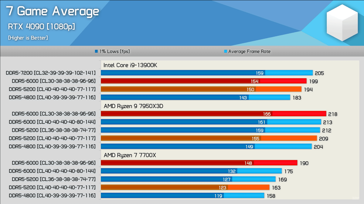
Hardware Unboxed
For both AMD processors, the RAM was operated at a maximum of 6000MHz, as the new AM5 firmware AGESA 1.0.0.7 was not yet available at the time of the test, which for the first time with the Ryzen 7000 processors also allows significantly higher clock rates for the RAM. For the Intel CPU, the YouTuber also provides measurement results with 7200MHz.
The video shows well that the performance gain depends strongly on the selected game. In Watch Dogs Legion, for example, all three processors benefit by 10 to 12 percent by switching from DDR5-4800 CL40 to DDR5-6000 CL40. In the next game, Horizon Zero Dawn, the FPS gain with the 13900K and the 7950X3D almost falls into the range of the measurement tolerances—only the 7700X,the weakest CPU in the test field, can benefit somewhat from the faster RAM. Another game in which all CPUs can register performance gains from faster RAM is Shadow of the Tomb Raider, which scales well with faster RAM or a faster CPU according to our own experience.
Across the seven games on average, it can be seen that the weakest processor benefits the most from higher RAM clock speeds. Just switching from 4800MHz to 6000MHz increases the FPS by 11 percent on average, and optimizing the latencies from CL40 to CL30 results in a further performance gain of 9 to 12 percent. With the Ryzen 9 7950X3D, the performance difference between the fastest and slowest configuration is much more manageable at just 7 to 11 percent. Reason number one is that the CPU quite often runs into the GPU limit. Reason two is that the X3D processor has a significantly larger L3 cache than, for example, the 7700X and therefore there are fewer accesses to the main memory.
The 13900K shows a similar picture to the 7950X3D. By switching from DDR5-4800 CL40 to DDR5-6000 CL30, the FPS increases on average by just 8 to 9 percent. The even faster RAM with 7200MHz at CL32 can bring out another 3 percent, a difference that is measurable but not really noticeable.
DDR4: How much extra performance does XMP or EXPO bring in games?
A few years ago, we examined a similar comparison with DDR4 RAM and, in particular, the influence of latencies. In the following table we have listed all the RAM speeds and latencies we tested:
| RAM specification | Latencies |
|---|---|
| 2666 MHz CL19-19-43 | ~ 14.25 ns |
| 3000 MHz CL16-18-38 | ~ 10.67 ns |
| 3000 MHz CL14-14-14-34 | ~ 9.33 ns |
| 3200 MHz CL16-18-18-38 | ~ 10.00 ns |
| 3200 MHz CL14-14-14-34 | ~ 8.75 ns |
| 3600 MHz CL18-22-42 | ~ 10.00 ns |
| 3600 MHz CL16-16-36 | ~ 8.89 ns |
| 3800 MHz CL18-22-22-42 | ~ 9.47 ns |
| 4000 MHz CL18-22-22-42 | ~ 9.00 ns |
| 4000 MHz CL17-17-37 | ~ 8.50 ns |
| 4266 MHz CL18-26-26-46 | ~ 8.44 ns |
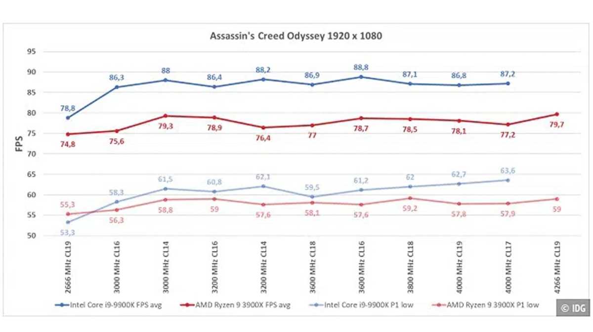
Our tests showed an almost identical picture. The example of Assassin’s Creed Odyssey shows that there are games where we quickly run into the GPU limit and therefore only benefit slightly from faster RAM. Even with a RAM clock of 3000MHz at CL14, we were able to measure just as many FPS with both test CPUs within the measurement tolerances as with a RAM clock of 3600MHz or even 4000MHz.
F1 2019, on the other hand, is an example where it is not only the RAM clock that matters, but also tight latencies. The Intel CPU in particular benefits significantly from optimized timings. With AMD, on the other hand, the drop in FPS values from 3800MHz is noticeable. From this RAM clock onwards, the RAM (real clock), the memory controller, and the Infinity Fabric no longer work in a 1:1:1 ratio, but in a 2:1:1 ratio, which causes the performance to plummet.
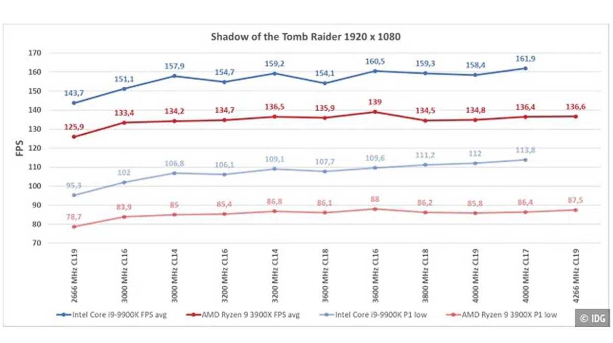
IDG
Shadow of the Tomb Raider is another example of how faster RAM brings greater performance gains, predominantly in the lower clock range.
IDG
DDR4 vs. DDR5 memory with Core i9-12900K
Whether you should go with DDR4 or DDR5 RAM is only relevant with the Intel processors of the 12th and 13th Core generation. AMD does not offer processors whose memory controller supports both memory types. We took the Core i9-12900K as an example for our test in 12 games and tested it with different clock rates:
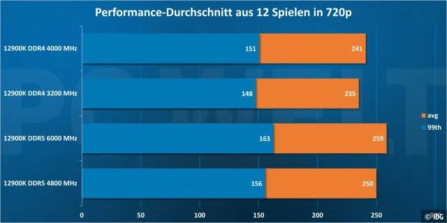
Sebastian Schenzinger
During the tests in the CPU limit, we were able to determine differences between DDR4 and DDR5 memory, but they were not really big. In the meantime, however, new DDR5 modules are available, which offer significantly better timings than when the new RAM standard was released.
How to find the clock rates and change them in the BIOS
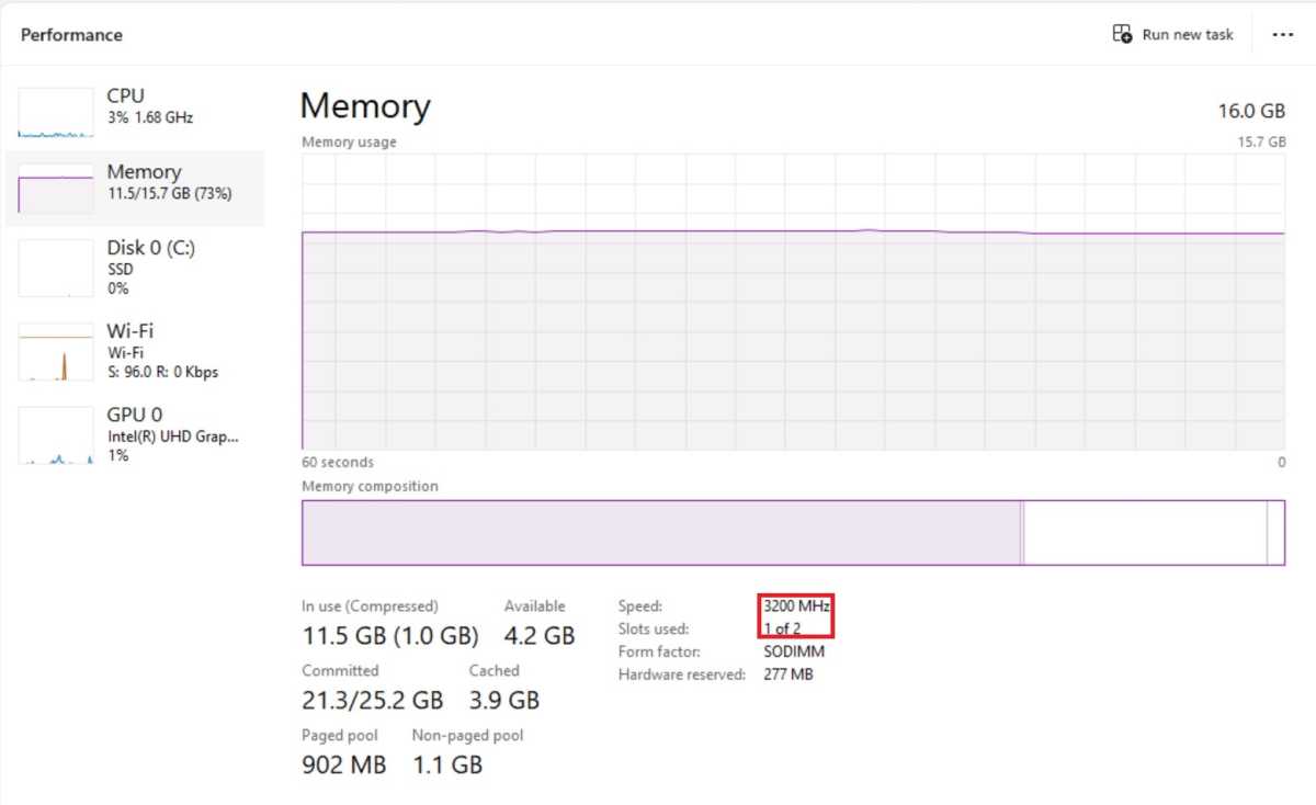
Finding out the current RAM clock is very easy with a current version of Windows 10 or Windows 11. To do this, open the Task Manager (Ctrl + Shift + Esc) and switch to the Performance tab. With the window maximized and the RAM selected, the speed can be easily read. The number of RAM modules installed and the number of available slots are also visible. From this it can be concluded whether the RAM is working in dual channel or not.
If you want to activate an XMP or EXPO, this can be done quickly in the BIOS. All you have to do is activate the correct memory profile (see picture below). Note: With AMD’s AM4 motherboards, the term “D.O.C.P.” is common here.
To do this, start your PC and press either the F2 or Del key during startup to enter the BIOS. There you activate the XMP, which can be found under the Overclocking Settings. Sometimes it is even possible that your main memory is equipped with several profiles—in this case, of course, you have the choice. Then confirm the changes you have made and restart the PC. In the task manager you can then check whether the set clock is present. If you cannot select XMP, EXPO, or D.O.C.P. in the BIOS, your RAM or motherboard does not support this function.